
Today, we are going to carry out a simple experiment using logic ICs to apply De Morgan First and Second Laws. They state that:
– the negation of a disjunction is the conjunction of the negations
– the negation of a conjunction is the disjunction of the negations
Wikipedia
Let’s keep the theory in the background and dive into the fun part! For this experiment, we need the following components:
- Logic OR gate – 7432
- Logic AND gate – 7408
- Logic NOT gate – 7404
- 2x 330ohms resistors
- BCD switch
- Breadboard + jumper wires
- 5V 0.5A power supply
We will split our experiment into two; first we show that \overline{ \left ( A + B \right )} = \overline{A} \cdot \overline{B}, and afterwards we show that \overline{ \left ( A \cdot B \right )} = \overline{A} + \overline{B}.
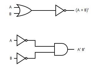
First Law – (A+B)’ = A’B’
For our first experiment we will set up the circuit as shown in the schematic below (Circuit 1). We will use the BCD switch to input four different bit combinations; 00, 01, 10, and 11. I used a logic analyzer to monitor the input and output values.
Jotting the input and output in a truth table will give us the following:
| A | B | A + B | (A + B)’ |
|---|---|---|---|
| 0 | 0 | 0 | 1 |
| 0 | 1 | 1 | 0 |
| 1 | 0 | 1 | 0 |
| 1 | 1 | 1 | 0 |
| A | B | A’ | B’ | A’B’ |
|---|---|---|---|---|
| 0 | 0 | 1 | 1 | 1 |
| 0 | 1 | 1 | 0 | 0 |
| 1 | 0 | 0 | 1 | 0 |
| 1 | 1 | 0 | 0 | 0 |
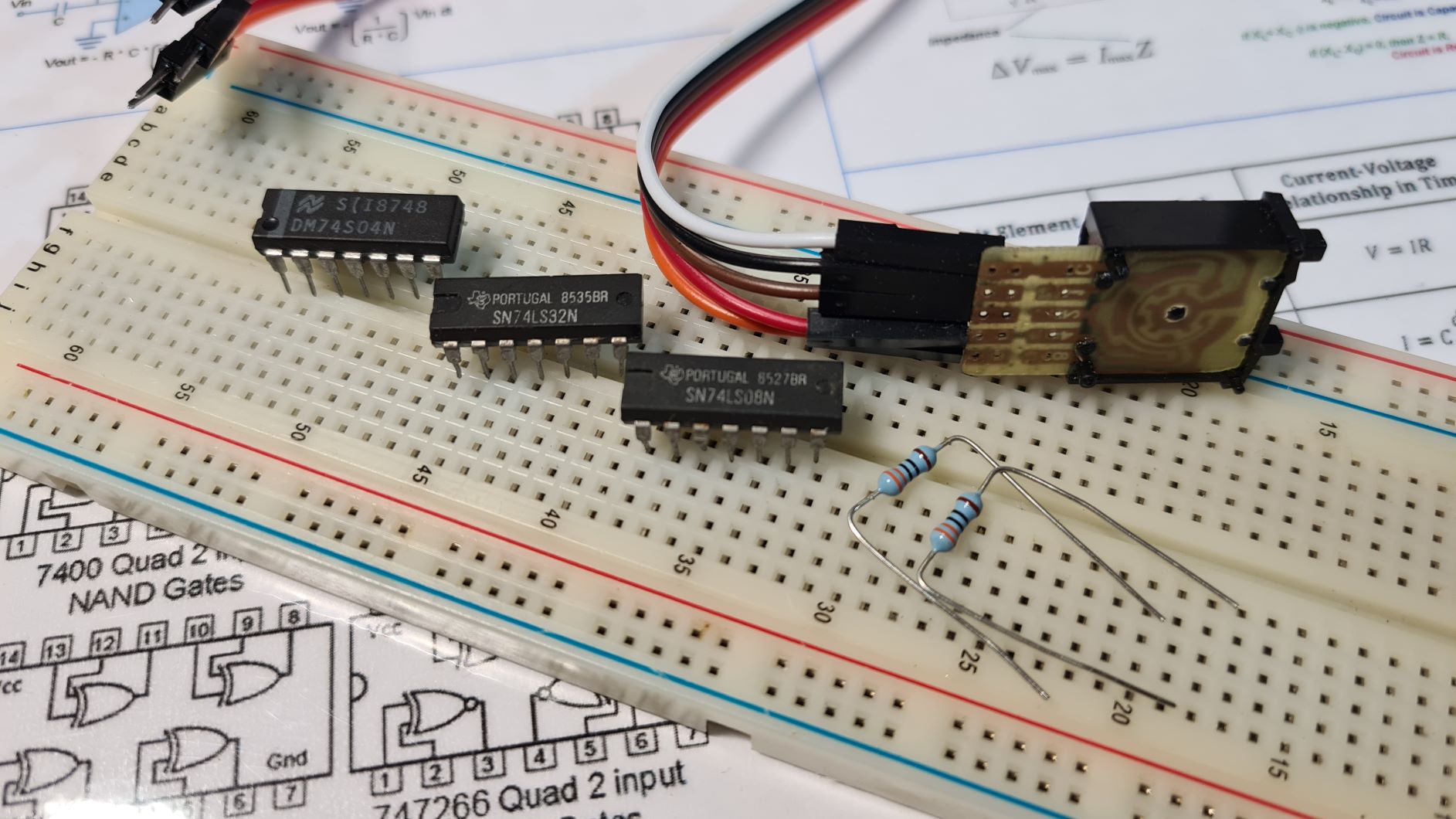
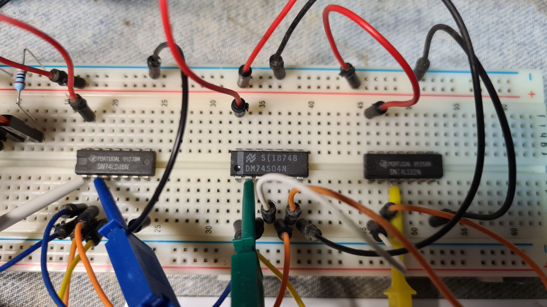
In my experiment, I connected both circuits, 1 and 2, on my breadboard, used the same input bits and confirmed that the output from circuit 1 is equal to circuit 2. The photo below shows my setup.
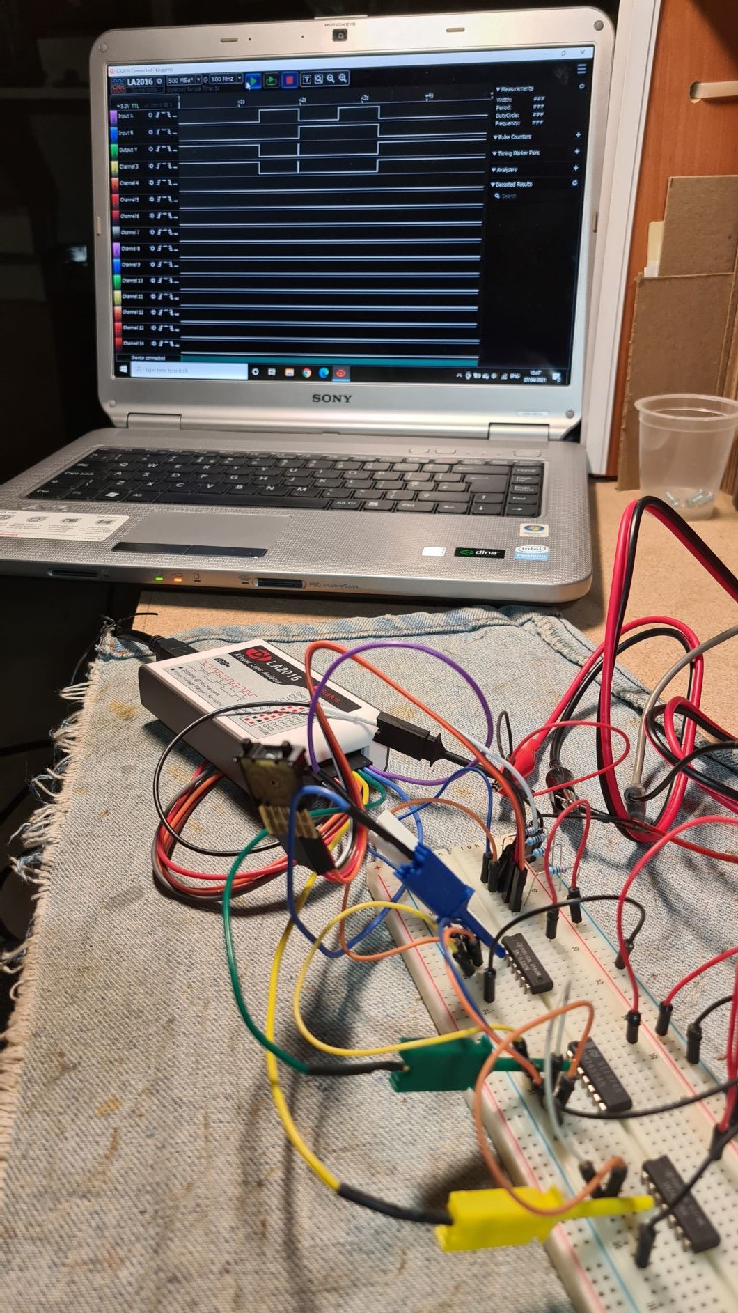
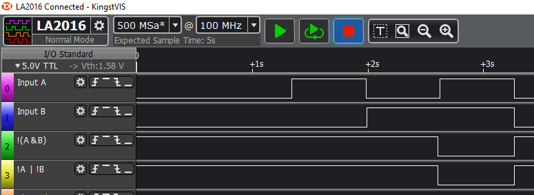
The logic analyzer output is detailed in the figure below.
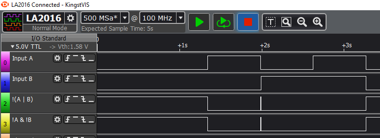
Channels 0 and 1 are the input bits, while channels 2 and 3 are the output from circuits 1a and 1b respectively. As one can see from the results obtained, both circuits produced same results despite the different logic circuit. That is, the output is HIGH (+5V) when both inputs are LOW (0V). Note that the spike on channel 2 and 3 at the 2nd second is due to the fact that during the increment from 01 to 10, the most significant bit took few milliseconds more to switch from 0 to 5V, thus there was a split second when both inputs were 0.
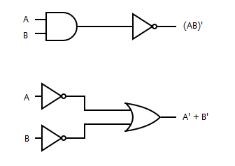
Second Law – (AB)’ = A’ + B’
Our second experiment is similar to the first but this time we swap the AND and OR logic gates as shown in circuits 2a and 2b.
Using the logic above, we can plot the output on a truth table as follows:
| A | B | A B | (A B)’ |
|---|---|---|---|
| 0 | 0 | 0 | 1 |
| 0 | 1 | 0 | 1 |
| 1 | 0 | 0 | 1 |
| 1 | 1 | 1 | 0 |
| A | B | A’ | B’ | A’+ B’ |
|---|---|---|---|---|
| 0 | 0 | 1 | 1 | 1 |
| 0 | 1 | 1 | 0 | 1 |
| 1 | 0 | 0 | 1 | 1 |
| 1 | 1 | 0 | 0 | 0 |
The photo below shows my setup, with all three logic IC, 7408 (AND), 7404 (NOT), and 7432 (OR), connected to my power source and logic analyzer.
Similarly, I connected my logic analyzer to the input and output pins and rotated the BCD from 0 to 3. The output is shown in the figure below.
Channels 2 and 3 are the outputs obtained for the 4 different input 2 bit combination (channels 0 and 1). We can see that the output is always HIGH (+5V) except when both inputs are HIGH.
Thus, we showed De Morgan’s theorem in practice using digital logic gates and basic TTL circuitry. This becomes handy when designing circuits to maximizes the utilization of all gates at hand. That is, you can utilize unused AND gates to produce OR-like operations and vice-versa!